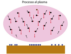
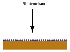
Applications of plasma enhanced chemical vapor deposition
Plasma Enhanced Chemical Vapour Deposition finds applications in numerous high-tech industries due to its ability to deposit uniform, high-quality films with excellent adhesion properties. Some key applications include:
Semiconductor Industry: PECVD is widely used for depositing dielectric films, such as silicon dioxide (SiO2) and silicon nitride (Si3N4), which serve as insulating layers and passivation coatings in integrated circuits.
Optical Coatings: The technique is employed to fabricate anti-reflective coatings, optical filters, and protective layers for lenses and display panels.
Solar Cells: PECVD plays a crucial role in the production of thin-film photovoltaic cells by depositing layers of amorphous silicon (a-Si) and transparent conductive oxides (TCOs).
Biomedical Devices: The ability to coat medical implants and devices with biocompatible films has made PECVD indispensable in the medical field.
Plasma Etching: PECVD can be integrated with plasma etching techniques to create precise microstructures and surface modifications for advanced applications.
With ongoing advancements in plasma technology and material science, Plasma Enhanced Chemical Vapour Deposition continues to evolve. Researchers are exploring novel precursor chemistries and advanced plasma configurations to further improve film properties and deposition efficiency. Additionally, the integration of PECVD with emerging fields such as nanotechnology and flexible electronics is expected to drive innovation, paving the way for next-generation electronic and optical devices.